I Applied to the DigiKey Make ONE Challenge 2026 and Didn't Make It — What Was in My Submitted Development Log
Overview
This is a maker contest hosted by electronics distributor DigiKey. Entries were submitted by registering a project on ProtoPedia and filling out a Google Form. Any award would have led to an exhibition at Maker Faire Tokyo 2026.
The result: eliminated in the first round.
What I Submitted
I compiled the entire development log for the ReLow60 L-HE into a ProtoPedia project page — covering the full process of designing and building everything solo: circuits, metal fabrication drawings, firmware, and configuration tool.
Development log covering circuits, case, firmware, and configuration tool
I understood this contest to be asking “what did you build and how,” so I kept philosophical discussion to a minimum and focused on the process of measuring, comparing, and deciding. Below are excerpts from the key sections of the submission.
Archetype09 — Starting with a 9-Key Proof-of-Concept
Jumping straight to a 60-key PCB carried too much risk. I first designed a 9-key tester board called Archetype09 and started with sensor and bypass capacitor selection.
Comparing Three Hall Sensors
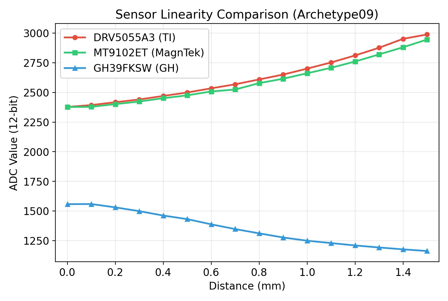
I mounted three Hall sensors — DRV5055A3 (Texas Instruments), MT9102ET (MagnTek), and GH39FKSW (GH) — on the same board and ran 8 tests covering noise, sensitivity, linearity, thermal drift, crosstalk, dynamic response, settling time, and scan rate.
The results showed that MT9102ET was overwhelmingly superior in thermal drift: ±9.2 LSB vs. ±33.8 LSB for DRV5055A3 and ±48.2 LSB for GH39FKSW.
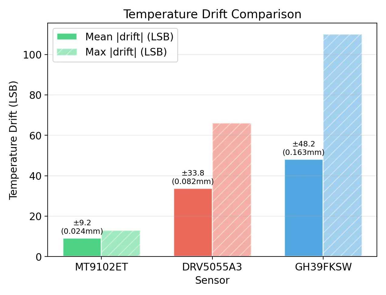
The MT9102ET is inferior in some noise and sensitivity metrics, but I chose it because keyboards experience temperature changes during use, making a small baseline shift the most practically significant factor. I selected based on actual use conditions, not raw catalog specifications.
Comparing Bypass Capacitors
A bypass capacitor is connected to the Hall sensor output pin to suppress high-frequency noise. Together with the sensor’s output impedance, this capacitor forms a low-pass filter that attenuates MUX switching noise and MCU clock noise. However, too large a capacitance can degrade the sensor’s response speed.
I therefore compared noise and settling time across four conditions: 0 nF (none), 1 nF, 2.2 nF, and 4.7 nF.
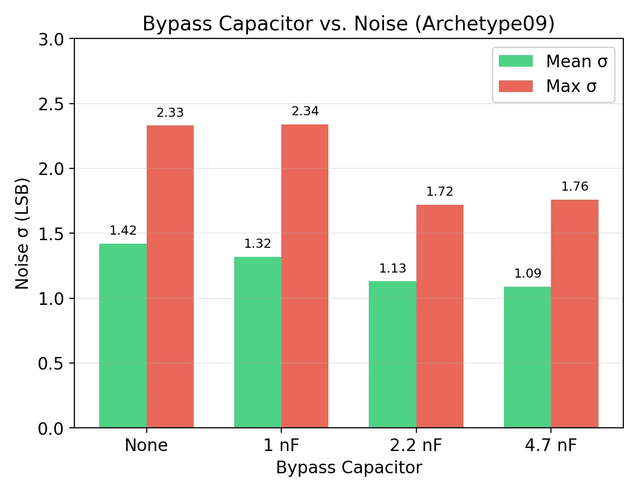
At 2.2 nF, noise was reduced by approximately 20%, achieving the same effect as 4.7 nF with no measurable impact on settling time (theoretical RC time constant τ = 10 Ω × 2.2 nF = 22 ns, well below the ADC conversion time of ~700 ns). I adopted 2.2 nF.
Difficulties Encountered with the Tester Board
The Archetype09 development itself was far from smooth. I documented everything transparently.
- All 5 boards failed to boot — The MCU (AT32F405) could not exit reset after power-on; USB and SWD were both unresponsive. After days of investigation and suspecting chip defects, a senior colleague pointed out that the NRST pull-up resistor was connected to GND instead of 3.3V — a schematic error.
- OLED not displaying — The AT32F405 has no Alternate Function mapped to the I2C SDA pin (PB5). Worked around temporarily with bit-bang I2C, later rerouted with a jumper wire to hardware I2C.
- MUX channel mapping offset — Missed the fact that the 4051’s channel numbers and pin numbers are non-sequential.
Every one of these failures informed the design of the ReLow60 main board.
Main Board — Scaling Up to ~70 Sensors
Using the knowledge gained from Archetype09, I designed the main board. It aggregates approximately 70 Hall sensors into the MCU’s ADC via 8 MUXes (SN74LV4051A-Q1).
The PCB is a 2-layer design with a GND pour on the back. Noise mitigation measures include separation of analog and digital signal traces, impedance-controlled USB differential pairs, and copper-free zones directly above sensors (to prevent copper from interfering with the Hall effect).
Scaling up introduced new challenges that were invisible at 9 keys: MUX switching settling time, crosstalk between adjacent channels, and loop time when scanning all keys simultaneously. Settling was resolved by adjusting the ADC sampling delay from 5 μs to 8 μs; crosstalk remained within spec at a maximum of 4 LSB.
The submission also covers the sheet-metal case design, firmware (a fork of libhmk), ReConf, bugs fixed through real-world testing, and distribution at Gaming Bazaar.
Reflections After the Rejection
Since I was eliminated in the first round, I received no comments from the judges. I don’t know the reason.
That said, the ProtoPedia page itself is now the best-organized record I have of my own development work. Despite the rejection, I’ve submitted it as a reference document in subsequent applications and used it to explain “what I’ve built” in conversations related to an AI grant program.
What I wrote for the contest has ended up doing work outside of it. Nothing I wrote was wasted.
A roundup of TiB, AI grant, DigiKey, and QWS applications
Test board for low-profile magnetic switches